Test: Applications of P-N Diode - NEET MCQ
25 Questions MCQ Test Physics Class 12 - Test: Applications of P-N Diode

The knee voltage of a-n junction diode is 0.8 V and the with of the depletion layer is 2 μm. What is the electric field in the depletion layer?
An electronic device which converts a.c power into d.c power is

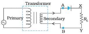
In a half wave rectifier, the secondary coil S of the transformer is connected to
A 50 Hz a.c. is rectified with full wave rectifier, what is the output frequency?
The conductivity of a photosensitive semiconductor
The current that exists in the circuit of a photodiode even when no visible light is made incident on it is called
For every 10°C increase in temperature, the reverse saturation current of a p-n junction will be increased by
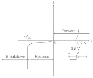
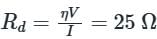
How does the dynamic resistance of diode vary with temperature?


Which of the following is a characteristic of a reverse-biased p-n junction?
A forward biased PN junction diode has a resistance of the order of
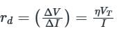
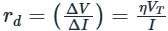
A diode whose terminal characteristics are related as Id = Is(eV/ηVT - 1) is biased at Id = 2 mA. Its dynamic resistance is:
(Given η = 2 and VT = 25 mV)
In a PN junction, with no external voltage, the electric field between the acceptor and the donor ions is called as
Choose the INCORRECT statement with regard to a forward biased pn diode.
A simple PN junction diode is fabricated using _______ semiconductor and can be used as a _________.
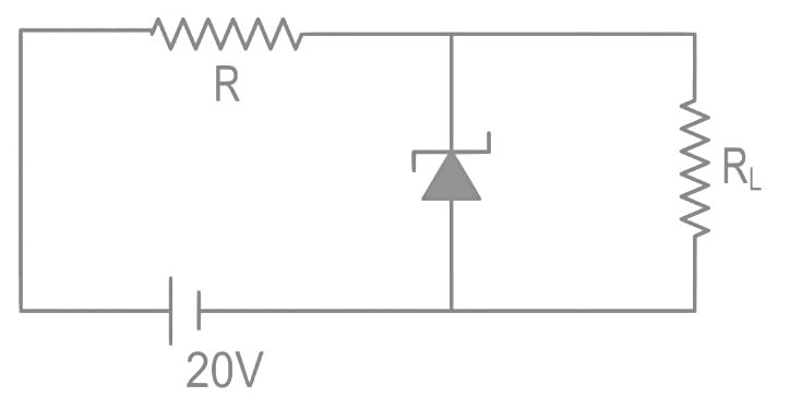
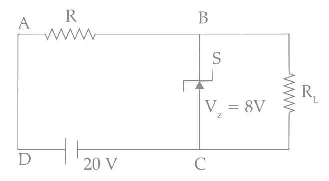
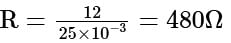
A 8 V Zener diode along with a series resistance R is connected across a 20 V supply (as shown in the figure). If the maximum Zener current is 25 mA, then the minimum value of R will be _______ Ω
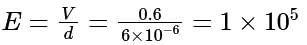
If the potential barrier across a p-n junction is 0.6 V. Then the electric field intensity, in the depletion region having the width of 6 x 10⁻⁶ m, will be __________ × 105 N/C.
In the ratio of the concentration of electrons that of holes in a semiconductor is 7/5 and the ratio of currents is 7/4 then what is the ratio of their drift velocities?
Mobility of electrons in a semiconductor is defined as the ratio of their drift velocity to the applied electric field. If for an n-type semiconductor, the density of electrons is 1019 m–3 and their mobility is 1.6 m2 /(V-s) then the resistivity of the semiconductor (since it is an n-type semiconductor contribution of holes is ignored) is close to
The electrical conductivity of a semiconductor increases when electromagnetic radiation of a wavelength shorter than 2480 nm is incident on it. The bandgap in (eV) for the semiconductor is
|
90 videos|420 docs|88 tests
|
Important Questions for Applications of P-N Diode
Applications of P-N Diode MCQs with Answers
Online Tests for Applications of P-N Diode Physics Class 12
|
© EduRev
|
Education Revolution
|


|


