


All Exams >
Electrical Engineering (EE) >
Power Electronics >
All Questions
All questions of Power Semiconductor Diodes & Transistors for Electrical Engineering (EE) Exam
A p-type semiconductor material is doped with ____________ impurities whereas a n-type semiconductor material is doped with __________ impurities- a)acceptor, donor
- b)acceptor, acceptor
- c)donor, donor
- d)donor, acceptor
Correct answer is option 'A'. Can you explain this answer?
A p-type semiconductor material is doped with ____________ impurities whereas a n-type semiconductor material is doped with __________ impurities
a)
acceptor, donor
b)
acceptor, acceptor
c)
donor, donor
d)
donor, acceptor
|
|
Disha Das answered |
Donor impurities denote an electron to the n-type material making it a electron majority carrier & vice-versa.

When the p-n junction diode is reversed biased, the width of the depletion region __________- a)increases
- b)decreases
- c)remains Constant
- d)none of the above mentioned
Correct answer is option 'A'. Can you explain this answer?
When the p-n junction diode is reversed biased, the width of the depletion region __________
a)
increases
b)
decreases
c)
remains Constant
d)
none of the above mentioned
|
|
Subham Chaudhary answered |
When reverse biased depletion layer increases until the breakdown value is reached.
The p-region has a greater concentration of __________ as compared to the n-region in a P-N junction.- a)holes
- b)electrons
- c)both holes & electrons
- d)phonons
Correct answer is option 'A'. Can you explain this answer?
The p-region has a greater concentration of __________ as compared to the n-region in a P-N junction.
a)
holes
b)
electrons
c)
both holes & electrons
d)
phonons

|
Shivam Sharma answered |
Holes are the majority charge carriers in p-type material.
In the p & n regions of the p-n junction the _________ & the ___________ are the minority charge carriers respectively.- a)holes, holes
- b)electrons, electrons
- c)holes, electrons
- d)electrons, holes
Correct answer is option 'D'. Can you explain this answer?
In the p & n regions of the p-n junction the _________ & the ___________ are the minority charge carriers respectively.
a)
holes, holes
b)
electrons, electrons
c)
holes, electrons
d)
electrons, holes
|
|
Jaya Rane answered |
Holes are the minority charge carriers in n-type material & vice-versa.
In the p & n regions of the p-n junction the _________ & the ___________ are the majority charge carriers respectively.- a)holes, holes
- b)electrons, electrons
- c)holes, electrons
- d)electrons, holes
Correct answer is option 'C'. Can you explain this answer?
In the p & n regions of the p-n junction the _________ & the ___________ are the majority charge carriers respectively.
a)
holes, holes
b)
electrons, electrons
c)
holes, electrons
d)
electrons, holes
|
|
Dishani Bose answered |
Holes are the majority charge carriers in p-type material & vice-versa.
In order to reduce the reverse recovery time of the diodes, __________ is carried out.- a)shortening of the length of the device
- b)platinum & gold doping
- c)antimony doping
- d)adding an extra silicon layer
Correct answer is option 'B'. Can you explain this answer?
In order to reduce the reverse recovery time of the diodes, __________ is carried out.
a)
shortening of the length of the device
b)
platinum & gold doping
c)
antimony doping
d)
adding an extra silicon layer
|
|
Aditya Basu answered |
Platinum & gold doping improves the performance of the devices.
In case of a practical p-n junction diode, the rise in the junction temperature ___________- a)decreases the width of the depletion region
- b)increases the barrier potential
- c)increases the width of the depletion region
- d)width of the depletion region increases but the barrier potential remains constant
Correct answer is option 'A'. Can you explain this answer?
In case of a practical p-n junction diode, the rise in the junction temperature ___________
a)
decreases the width of the depletion region
b)
increases the barrier potential
c)
increases the width of the depletion region
d)
width of the depletion region increases but the barrier potential remains constant
|
|
Ashwin Mukherjee answered |
The rise in temperature excites the charges, which go & recombine with the charges in the depletion region decreasing its width. Higher the temperature, lesser is the E.M.F required to turn on the device.
In the equilibrium state the barrier, potential across a unbiased germanium diode is __________- a)0.3 V
- b)0.7 V
- c)1.7 V
- d)0 V
Correct answer is option 'A'. Can you explain this answer?
In the equilibrium state the barrier, potential across a unbiased germanium diode is __________
a)
0.3 V
b)
0.7 V
c)
1.7 V
d)
0 V
|
|
Vaishnavi Singh answered |
Barrier potential is due to the charges that establish an electric field across the two junctions.
When reverse breakdown occurs in a diode- a)voltage increases & current is constant
- b)voltage increases & current also increases
- c)both are constant
- d)voltage is constant & current increases
Correct answer is option 'D'. Can you explain this answer?
When reverse breakdown occurs in a diode
a)
voltage increases & current is constant
b)
voltage increases & current also increases
c)
both are constant
d)
voltage is constant & current increases
|
|
Madhurima Das answered |
Recall the I-V curve of a diode in the 3rd quadrant.
In an AC-DC converter, a diode might be used as a- a)voltage source
- b)phase angle controller
- c)freewheeling Diode
- d)filter
Correct answer is option 'C'. Can you explain this answer?
In an AC-DC converter, a diode might be used as a
a)
voltage source
b)
phase angle controller
c)
freewheeling Diode
d)
filter
|
|
Sanjana Chopra answered |
In converters diodes are used to feed the energy back to the load in case of an inductive load.
The V-I Characteristics of the diode lie in the- a)1st & 2nd quadrant
- b)1st & 3rd quadrant
- c)1st & 4th quadrant
- d)Only in the 1st quadrant
Correct answer is option 'B'. Can you explain this answer?
The V-I Characteristics of the diode lie in the
a)
1st & 2nd quadrant
b)
1st & 3rd quadrant
c)
1st & 4th quadrant
d)
Only in the 1st quadrant
|
|
Sanjana Chopra answered |
First in the forward region & Third in the reverse biased mode.
The n-region has a greater concentration of _________ as compared to the p-region in a P-N junction diode.- a)holes
- b)electrons
- c)both holes & electrons
- d)phonons
Correct answer is option 'B'. Can you explain this answer?
The n-region has a greater concentration of _________ as compared to the p-region in a P-N junction diode.
a)
holes
b)
electrons
c)
both holes & electrons
d)
phonons
|
|
Jaya Rane answered |
Electrons are the majority charge carriers in n-type material.
Which of the below mentioned statements is false regarding a p-n junction diode?- a)Diode are uncontrolled devices
- b)Diodes are rectifying devices
- c)Diodes are unidirectional devices
- d)Diodes have three terminals
Correct answer is option 'D'. Can you explain this answer?
Which of the below mentioned statements is false regarding a p-n junction diode?
a)
Diode are uncontrolled devices
b)
Diodes are rectifying devices
c)
Diodes are unidirectional devices
d)
Diodes have three terminals
|
|
Ashwin Mukherjee answered |
Diode is a two terminal device, anode & cathode are the two terminals.
The peak inverse current IP for a power diode is given by the expression- a) IP=t + di/dt
- b)IP=t * log i
- c)IP=t * di/dt
- d)IP=t * ∫ t*i dt
Correct answer is option 'C'. Can you explain this answer?
The peak inverse current IP for a power diode is given by the expression
a)
IP=t + di/dt
b)
IP=t * log i
c)
IP=t * di/dt
d)
IP=t * ∫ t*i dt
|
|
Divya Nair answered |
The leakage current is the reveres recovery time (t) into the rate of change of current.
Which of the following is true in case of a forward biased p-n junction diode?- a)The positive terminal of the battery sucks electrons from the p-region
- b)The positive terminal of the battery injects electrons into the p-region
- c)The negative terminal of the battery sucks electrons from the p-region
- d)None of the above mentioned statements are true
Correct answer is option 'A'. Can you explain this answer?
Which of the following is true in case of a forward biased p-n junction diode?
a)
The positive terminal of the battery sucks electrons from the p-region
b)
The positive terminal of the battery injects electrons into the p-region
c)
The negative terminal of the battery sucks electrons from the p-region
d)
None of the above mentioned statements are true
|
|
Maulik Choudhury answered |
The diode is forward biased, positive is connected to p & vice-versa, as such batter provides EMF to drive electrons from n-region to p-region.
A diode is said to be reversed biased when the- a)cathode is positive with respect to the anode
- b)anode is positive with respect to the cathode
- c)cathode is negative with respect to the anode
- d)both cathode & anode are negative
Correct answer is option 'A'. Can you explain this answer?
A diode is said to be reversed biased when the
a)
cathode is positive with respect to the anode
b)
anode is positive with respect to the cathode
c)
cathode is negative with respect to the anode
d)
both cathode & anode are negative
|
|
Tarun Chawla answered |
K is positive w.r.t the A when the device is reversed biased.
In a Schottky diode, the aluminum metal acts as a __________- a)anode
- b)cathode
- c)gate
- d)common terminal
Correct answer is option 'A'. Can you explain this answer?
In a Schottky diode, the aluminum metal acts as a __________
a)
anode
b)
cathode
c)
gate
d)
common terminal
|
|
Prasad Saini answered |
The Al (Metal) always acts as the anode.
As compared to a p-n junction device of equal rating, the Schottky diode has- a)lower reverse voltage rating
- b)lower reverse leakage current
- c)higher Switching time
- d)higher cut-in voltage
Correct answer is option 'A'. Can you explain this answer?
As compared to a p-n junction device of equal rating, the Schottky diode has
a)
lower reverse voltage rating
b)
lower reverse leakage current
c)
higher Switching time
d)
higher cut-in voltage
|
|
Prisha Kulkarni answered |
Low reverse voltage rating is the only drawback against a p-n junction diode.
Which of the following is true in case of a power diode with R load?- a)I grows almost linearly with V
- b)I decays almost linearly with V
- c)I is independent of V
- d)I initial grows than decays
Correct answer is option 'A'. Can you explain this answer?
Which of the following is true in case of a power diode with R load?
a)
I grows almost linearly with V
b)
I decays almost linearly with V
c)
I is independent of V
d)
I initial grows than decays
|
|
Bijoy Nair answered |
R load therefore V and I are linear and in phase.
Power diode is __________- a)a three terminal semiconductor device
- b)a two terminal semiconductor device
- c)a four terminal semiconductor device
- d)a three terminal analog device
Correct answer is option 'B'. Can you explain this answer?
Power diode is __________
a)
a three terminal semiconductor device
b)
a two terminal semiconductor device
c)
a four terminal semiconductor device
d)
a three terminal analog device
|
|
Devansh Das answered |
It has two terminals anode and cathode same as that of a ordinary diode. In fact, a power diode is nothing but a signal diode with a extra layer.
A diode is said to be forward biased when the- a)cathode is positive with respect to the anode
- b)anode is positive with respect to the cathode
- c)anode is negative with respect to the anode
- d)both cathode & anode are positive
Correct answer is option 'B'. Can you explain this answer?
A diode is said to be forward biased when the
a)
cathode is positive with respect to the anode
b)
anode is positive with respect to the cathode
c)
anode is negative with respect to the anode
d)
both cathode & anode are positive
|
|
Ashwin Mukherjee answered |
A is positive w.r.t the K when the device is forward biased.
If V & I are the forward voltage & current respectively, then the power loss across the diode would be- a)V/I
- b)V2 I2
- c)I2 V
- d)VI
Correct answer is option 'D'. Can you explain this answer?
If V & I are the forward voltage & current respectively, then the power loss across the diode would be
a)
V/I
b)
V2 I2
c)
I2 V
d)
VI
|
|
Sharmila Bajaj answered |
If V is in reference to voltage, it represents the potential difference between two points in an electrical circuit. It is measured in volts (V) and is responsible for the flow of electric current.
When the p-n junction diode is forward biased, the width of the depletion region __________- a)increases
- b)decreases
- c)remains Constant
- d)increases than Decreases
Correct answer is option 'B'. Can you explain this answer?
When the p-n junction diode is forward biased, the width of the depletion region __________
a)
increases
b)
decreases
c)
remains Constant
d)
increases than Decreases
|
|
Sanaya Basu answered |
When forward biased depletion layer decreases & finally it collapses to allow the current flow.
In a Schottky diode, the silicon layer acts as a _____________- a)anode
- b)cathode
- c)gate
- d)common terminal
Correct answer is option 'B'. Can you explain this answer?
In a Schottky diode, the silicon layer acts as a _____________
a)
anode
b)
cathode
c)
gate
d)
common terminal
|
|
Megha Datta answered |
The metal acts as the anode and the semiconductor as a cathode.
In a certain power electronics application, it is required that the voltage at the load terminals is to be kept within a certain range of voltages only. Among the device listed below, which would be the most ideal choice for this application?- a)P-n junction diode
- b)Schottky diode
- c)Zener diode
- d)Fast recover diode
Correct answer is option 'C'. Can you explain this answer?
In a certain power electronics application, it is required that the voltage at the load terminals is to be kept within a certain range of voltages only. Among the device listed below, which would be the most ideal choice for this application?
a)
P-n junction diode
b)
Schottky diode
c)
Zener diode
d)
Fast recover diode
|
|
Sanchita Sharma answered |
Zener diode is used as a voltage regulating device.
When a physical contact between a p-region & n-region is established which of the following is most likely to take place?- a)Electrons from N-region diffuse to P-region
- b)Holes from P-region diffuse to N-region
- c)Both of the above mentioned statements are true
- d)Nothing will happen
Correct answer is option 'C'. Can you explain this answer?
When a physical contact between a p-region & n-region is established which of the following is most likely to take place?
a)
Electrons from N-region diffuse to P-region
b)
Holes from P-region diffuse to N-region
c)
Both of the above mentioned statements are true
d)
Nothing will happen
|
|
Sanskriti Bajaj answered |
And an n-region occurs in a semiconductor, it forms a p-n junction.
A Schottky diode can be switchd off much faster than an equivalent p-n junction diode due to its- a)higher operating frequency
- b)no recombination of charges
- c)more compact structure
- d)None of the mentioned
Correct answer is option 'B'. Can you explain this answer?
A Schottky diode can be switchd off much faster than an equivalent p-n junction diode due to its
a)
higher operating frequency
b)
no recombination of charges
c)
more compact structure
d)
None of the mentioned
|
|
Kalyan Patel answered |
Due to the metal-silicon junction there are no stored charges, hence no reverse recovery time due to which the switching is faster.
Which of the following is true in case of an unbiased p-n junction diode?- a)Diffusion does not take place
- b)Diffusion of electrons & holes goes on infinitely
- c)There is zero electrical potential across the junctions
- d)Charges establish an electric field across the junctions
Correct answer is option 'D'. Can you explain this answer?
Which of the following is true in case of an unbiased p-n junction diode?
a)
Diffusion does not take place
b)
Diffusion of electrons & holes goes on infinitely
c)
There is zero electrical potential across the junctions
d)
Charges establish an electric field across the junctions
|
|
Subham Chaudhary answered |
A potential difference is established across the junctions due to recombination of holes & electrons. This growing filed (barrier potential) stops the further diffusion.
If the doping levels of the semiconductor is increased, then the width of the depletion layer- a)increases
- b)decreases
- c)is unchanged
- d)keeps oscillating
Correct answer is option 'B'. Can you explain this answer?
If the doping levels of the semiconductor is increased, then the width of the depletion layer
a)
increases
b)
decreases
c)
is unchanged
d)
keeps oscillating
|
|
Shivam Ghosh answered |
Higher the doping, more the number of charge carrier available to neutralize the opposite charges on the junction.
Even after the forward current reduces to zero value, a practical diode continues to conduct in the reverse direction for a while due to the- a)resistance of the diode
- b)high junction temperature
- c)stored charges in the depletion region
- d)none of the mentioned
Correct answer is option 'C'. Can you explain this answer?
Even after the forward current reduces to zero value, a practical diode continues to conduct in the reverse direction for a while due to the
a)
resistance of the diode
b)
high junction temperature
c)
stored charges in the depletion region
d)
none of the mentioned
|
|
Sneha Bose answered |
Explanation:
When a diode is forward-biased, it allows the flow of current through it. However, once the forward current reduces to zero, a practical diode does not immediately stop conducting in the reverse direction. This is due to the presence of stored charges in the depletion region of the diode.
Depletion Region:
The depletion region is a region in a diode where there are no majority charge carriers (electrons in the N-region and holes in the P-region). It forms due to the diffusion of charge carriers across the junction when a diode is not biased. In this region, there are immobile ions and fixed charges.
Stored Charges:
When a diode is forward-biased, the depletion region becomes very narrow, and the majority charge carriers (electrons and holes) cross the junction and contribute to the forward current. However, when the forward current reduces to zero, the depletion region expands again, and the majority charge carriers are no longer present in the region.
However, there are still immobile ions and fixed charges in the depletion region. These charges are responsible for creating an electric field across the junction. When the diode is reverse-biased, the electric field pushes the minority carriers (minority carriers are electrons in P-region and holes in N-region) towards the junction.
Conduction in Reverse Direction:
The stored charges in the depletion region create a potential barrier that needs to be overcome for the diode to conduct in the reverse direction. This potential barrier prevents the flow of current initially. However, due to the thermal energy, some minority carriers acquire enough energy to overcome the potential barrier and cross the junction, resulting in a small reverse current.
This small reverse current is known as the reverse saturation current and is typically very small compared to the forward current. It is also temperature-dependent, increasing with temperature.
Therefore, even after the forward current reduces to zero, a practical diode continues to conduct in the reverse direction for a while due to the stored charges in the depletion region. As the stored charges gradually dissipate, the reverse current decreases, and the diode eventually stops conducting in the reverse direction.
Conclusion:
The correct answer is option C - stored charges in the depletion region. These stored charges create a potential barrier that allows the diode to conduct in the reverse direction even after the forward current reduces to zero.
Which of the following are/is the majority charge carriers in a Schottky diode?- a)Holes
- b)Electrons
- c)Both holes & Electrons carry equal current
- d)None of the mentioned
Correct answer is option 'B'. Can you explain this answer?
Which of the following are/is the majority charge carriers in a Schottky diode?
a)
Holes
b)
Electrons
c)
Both holes & Electrons carry equal current
d)
None of the mentioned
|
|
Partho Saha answered |
The metal has no holes hence major(almost full) current flows due to the electrons only.
A Schottky diode _____- a)has current flow due to holes only
- b)has no reverse recovery time
- c)has large amount of storage charges
- d)has zero cut-in voltage
Correct answer is option 'B'. Can you explain this answer?
A Schottky diode _____
a)
has current flow due to holes only
b)
has no reverse recovery time
c)
has large amount of storage charges
d)
has zero cut-in voltage
|
|
Yashvi Shah answered |
Due to the metal-silicon junction there are no stored charges hence, no reverse recovery time, due to which the switching is faster.
To make a signal diode suitable for high current & high voltage carrying applications with minimum losses, ________- a)a lightly doped n layer is grown between the two p & n layers
- b)a heavily doped n layer is grown between the two p & n layers
- c)a lightly doped p layer is grown between the two p & n layers
- d)a heavily doped p layer is grown between the two p & n layers
Correct answer is option 'A'. Can you explain this answer?
To make a signal diode suitable for high current & high voltage carrying applications with minimum losses, ________
a)
a lightly doped n layer is grown between the two p & n layers
b)
a heavily doped n layer is grown between the two p & n layers
c)
a lightly doped p layer is grown between the two p & n layers
d)
a heavily doped p layer is grown between the two p & n layers
|
|
Pranab Basu answered |
The above process simply the one used to manufacture power diodes.
Which of the following diodes uses a metal-semiconductor junction?- a)General purpose diodes
- b)Fast recovery diodes
- c)Schottky diode
- d)None of the mentioned
Correct answer is option 'C'. Can you explain this answer?
Which of the following diodes uses a metal-semiconductor junction?
a)
General purpose diodes
b)
Fast recovery diodes
c)
Schottky diode
d)
None of the mentioned
|
|
Ishan Saini answered |
Schottky diode uses a Al-Semiconductor junction.
Schottky diodes are also called as- a)metal diode
- b)hot carrier diode
- c)signaling diode
- d)easy turn on diode
Correct answer is option 'B'. Can you explain this answer?
Schottky diodes are also called as
a)
metal diode
b)
hot carrier diode
c)
signaling diode
d)
easy turn on diode
|
|
Aaditya Choudhary answered |
Due to the metal used to carry the current, it is also called as a hot carrier diode.
In a Schottky diode, the silcon is usually- a)N-type
- b)P-type
- c)un-doped semiconductor
- d)silicon is not used
Correct answer is option 'A'. Can you explain this answer?
In a Schottky diode, the silcon is usually
a)
N-type
b)
P-type
c)
un-doped semiconductor
d)
silicon is not used
|
|
Disha Das answered |
Usually only n-type silicon is used because the p-type has certain limitations.
In the equilibrium state, the barrier potential across a unbiased silicon diode is _________- a)0.3 V
- b)0.7 V
- c)1.3 V
- d)0 V
Correct answer is option 'B'. Can you explain this answer?
In the equilibrium state, the barrier potential across a unbiased silicon diode is _________
a)
0.3 V
b)
0.7 V
c)
1.3 V
d)
0 V
|
|
Saumya Basak answered |
Barrier potential is due to the charges that establish an electric field across the two junctions.
Zener diodes allow a current to flow in the reverse direction, when the- a)voltage reaches above a certain value
- b)temperature reaches above a certain value
- c)current always flows in the reverse direction only
- d)current cannot flow in the reverse direction
Correct answer is option 'A'. Can you explain this answer?
Zener diodes allow a current to flow in the reverse direction, when the
a)
voltage reaches above a certain value
b)
temperature reaches above a certain value
c)
current always flows in the reverse direction only
d)
current cannot flow in the reverse direction
|
|
Prateek Mehra answered |
Zener diode has voltage regulating property. When voltage reaches above a certain value (Zener voltage), current starts to flow in the reverse direction.
For a p-n junction diode, the peak inverse current & the reverse recovery time are dependent on- a)inverse voltage
- b)forward Voltage
- c)di/dt
- d)all of the above mentioned
Correct answer is option 'C'. Can you explain this answer?
For a p-n junction diode, the peak inverse current & the reverse recovery time are dependent on
a)
inverse voltage
b)
forward Voltage
c)
di/dt
d)
all of the above mentioned
|
|
Rajesh Saha answered |
It only depends upon the number stored charges which depends upon the rate of change of current.
The power loss in which of the following cases would be the maximum?- a)When both V & I are minimum
- b)When both V & I are maximum
- c)When only V is maximum
- d)When only I is maximum
Correct answer is option 'B'. Can you explain this answer?
The power loss in which of the following cases would be the maximum?
a)
When both V & I are minimum
b)
When both V & I are maximum
c)
When only V is maximum
d)
When only I is maximum
|
|
Prisha Iyer answered |
P=VI Hence, it would be maximum when both V and I are maximum.
An ideal power diode must have- a)low forward current carrying capacity
- b)large reverse breakdown voltage
- c)high ohmic junction resistance
- d)high reverse recovery time
Correct answer is option 'B'. Can you explain this answer?
An ideal power diode must have
a)
low forward current carrying capacity
b)
large reverse breakdown voltage
c)
high ohmic junction resistance
d)
high reverse recovery time
|
|
Gaurav Chauhan answered |
Large reverse breakdown voltage is desirable whereas others will increases the losses.
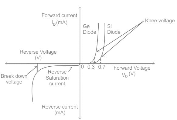
The barrier voltage for germanium is _________ at 25°C.- a)0.3 V
- b)0.7 V
- c)0 V
- d)infinity
Correct answer is option 'A'. Can you explain this answer?
The barrier voltage for germanium is _________ at 25°C.
a)
0.3 V
b)
0.7 V
c)
0 V
d)
infinity

|
EduRev GATE answered |
Barrier voltage
The minimum voltage required by a diode to conduct is known as barrier voltage.
It is also known as the cut-in voltage or knee voltage.
The barrier potential of the "Germanium" diode is 0.3 V.
The barrier potential of the "Silicon" diode is 0.7 V.
Above the knee voltage, the diode conducts and the forward current from p to n flows in the diode.
Which of the below mentioned statements is false regarding Schottky diodes?- a)Schottky diodes have a Al-Silicon junction
- b)There is no storage of charges in a Schottky diode
- c)The majority charge carriers in a Schottky diode are holes
- d)Schottky diodes can be switched off faster than a p-n junction diode of the same rating
Correct answer is option 'C'. Can you explain this answer?
Which of the below mentioned statements is false regarding Schottky diodes?
a)
Schottky diodes have a Al-Silicon junction
b)
There is no storage of charges in a Schottky diode
c)
The majority charge carriers in a Schottky diode are holes
d)
Schottky diodes can be switched off faster than a p-n junction diode of the same rating
|
|
Madhurima Das answered |
The majority charge carriers in a Schottky diode are electrons not holes.
A power diode with small softness factor (S-factor) has- a)small oscillatory over voltages
- b)large oscillatory over voltages
- c)large peak reverse current
- d)small peak reverse current
Correct answer is option 'B'. Can you explain this answer?
A power diode with small softness factor (S-factor) has
a)
small oscillatory over voltages
b)
large oscillatory over voltages
c)
large peak reverse current
d)
small peak reverse current
|
|
Devansh Das answered |
Peak reverse current is independent of S-factor smaller the value of S-factor larger the oscillatory over voltage.
Shown below is the diagram of an ideal super diode. When the input voltage Vin is negative, then the output voltage Vout = ?
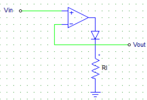
- a)Vout/Vin
- b)Vin
- c)0
- d)Vin * Rl
Correct answer is option 'C'. Can you explain this answer?
Shown below is the diagram of an ideal super diode. When the input voltage Vin is negative, then the output voltage Vout = ?
a)
Vout/Vin
b)
Vin
c)
0
d)
Vin * Rl

|
Anirban Khanna answered |
When the input voltage is negative, there would be a negative voltage on the diode so it works like an open circuit. Hence no current flows through the load and Vout is zero.
Shown below is the diagram of an ideal super diode. When the input voltage Vin is positive, then the output voltage Vout = ?
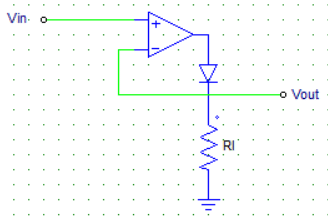
- a)Vout/Vin
- b)Vin
- c)0
- d)Vin * Rl
Correct answer is option 'B'. Can you explain this answer?
Shown below is the diagram of an ideal super diode. When the input voltage Vin is positive, then the output voltage Vout = ?
a)
Vout/Vin
b)
Vin
c)
0
d)
Vin * Rl
|
|
Ameya Nambiar answered |
Input is positive, hence it is amplified by the operational amplifier which switches the diode on. Current flows through the load & because of the feedback, the output voltage is equal to the input voltage.
A Schottky diode has __________- a)A gate terminal
- b)Aluminum-silicon junction
- c)Platinum gold junction
- d)Germanium-Arsenide junction
Correct answer is option 'B'. Can you explain this answer?
A Schottky diode has __________
a)
A gate terminal
b)
Aluminum-silicon junction
c)
Platinum gold junction
d)
Germanium-Arsenide junction
|
|
Sanchita Choudhary answered |
Introduction:
A Schottky diode is a type of diode that is formed by a metal-semiconductor junction rather than a p-n junction. It is named after the German physicist Walter H. Schottky. The metal-semiconductor junction is typically made of aluminum-silicon, which gives the diode its unique characteristics and advantages.
Explanation:
The correct answer is option B, which states that a Schottky diode has an aluminum-silicon junction. Let's understand why this is the correct answer.
What is a Schottky Diode?
A Schottky diode is a semiconductor device that allows current to flow in one direction while offering very low forward voltage drop and fast switching characteristics. It is widely used in various electronic circuits, such as rectifiers, voltage clamps, and high-frequency applications.
Metal-Semiconductor Junction:
A Schottky diode is formed by the junction of a metal (typically aluminum) and a semiconductor (usually silicon). This metal-semiconductor junction is known as the Schottky barrier. Unlike a regular diode, which uses a p-n junction, the Schottky diode utilizes the rectifying properties of the metal-semiconductor junction.
Aluminum-Silicon Junction:
In a Schottky diode, the metal used is typically aluminum, and the semiconductor used is silicon. Aluminum is chosen as the metal due to its low work function and good rectifying characteristics. Silicon is selected as the semiconductor material due to its widespread availability, excellent electrical properties, and compatibility with aluminum.
Advantages of Aluminum-Silicon Junction:
- Low Forward Voltage Drop: The aluminum-silicon junction in a Schottky diode exhibits a lower forward voltage drop compared to a regular diode. This results in lower power losses and improved efficiency.
- Fast Switching Speed: The absence of a depletion region in the metal-semiconductor junction allows for faster switching characteristics. This makes Schottky diodes suitable for high-frequency applications.
- Low Reverse Recovery Time: Schottky diodes have a very short reverse recovery time, which means they can quickly transition from the ON state to the OFF state. This makes them ideal for applications that require fast rectification.
Conclusion:
In summary, a Schottky diode has an aluminum-silicon junction, which is responsible for its unique characteristics and advantages. The aluminum-silicon junction provides a low forward voltage drop, fast switching speed, and low reverse recovery time, making Schottky diodes widely used in various electronic applications.
Chapter doubts & questions for Power Semiconductor Diodes & Transistors - Power Electronics 2025 is part of Electrical Engineering (EE) exam preparation. The chapters have been prepared according to the Electrical Engineering (EE) exam syllabus. The Chapter doubts & questions, notes, tests & MCQs are made for Electrical Engineering (EE) 2025 Exam. Find important definitions, questions, notes, meanings, examples, exercises, MCQs and online tests here.
Chapter doubts & questions of Power Semiconductor Diodes & Transistors - Power Electronics in English & Hindi are available as part of Electrical Engineering (EE) exam.
Download more important topics, notes, lectures and mock test series for Electrical Engineering (EE) Exam by signing up for free.
Power Electronics
5 videos|67 docs|46 tests
|
|
© EduRev
|
Education Revolution
|


|


Signup to see your scores
go up within 7 days!
Access 1000+ FREE Docs, Videos and Tests
Takes less than 10 seconds to signup